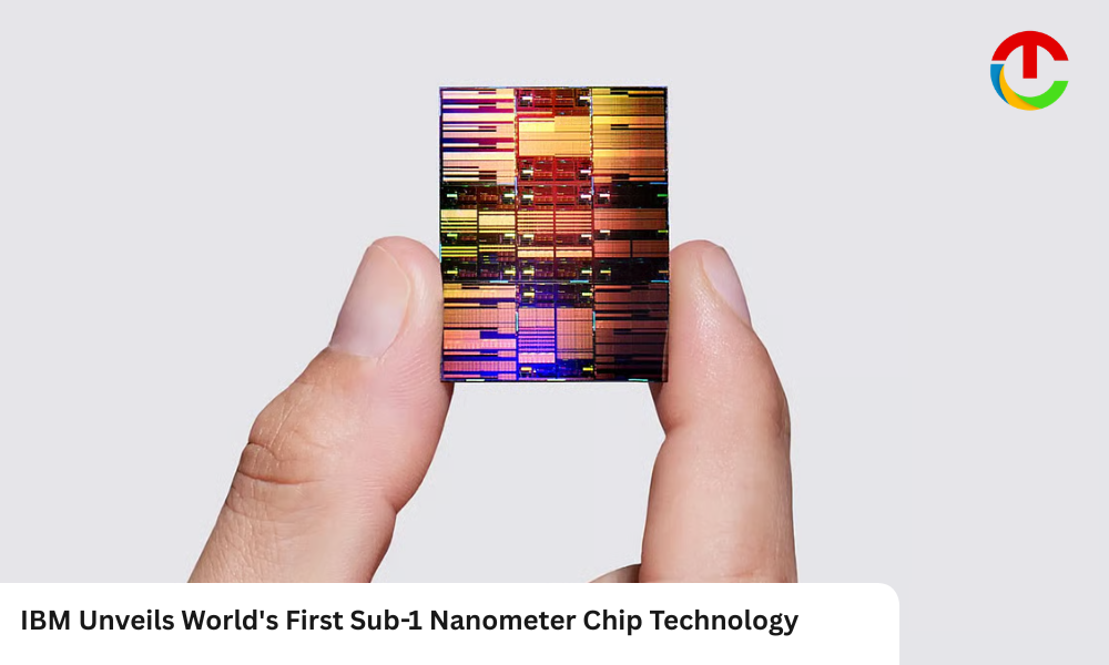
IBM has announced a major breakthrough in semiconductor technology with the introduction of the world’s first sub-1 nanometer (0.7 nm or 7 angstrom) nanometer chip technology. The innovation marks a significant advancement for the semiconductor industry as it pushes beyond the conventional limits of chip scaling.
The newly developed chip integrates nearly 100 billion transistors onto a fingernail-sized chip—almost double the transistor density of IBM’s 2 nm chip introduced in 2021. Powered by an innovative three-dimensional transistor architecture known as Nanostack, the technology is designed to deliver substantial improvements in computing performance while reducing energy consumption.
Nanostack Redefines Chip Architecture
At the heart of the breakthrough is IBM’s new Nanostack architecture, the industry’s first known three-dimensional Nanometer Chip Technology -based transistor design. Unlike traditional chip layouts, Nanostack vertically stacks transistors, enabling significantly higher transistor density and allowing different materials to be used across layers for optimized performance and power efficiency.
IBM researchers successfully demonstrated the architecture through advanced CMOS integration, dual-channel engineering, and functional circuit operations, validating that the technology is capable of supporting real-world computing applications.
Faster AI and Energy-Efficient Computing
According to IBM, the new sub-1 nm technology is projected to deliver up to 50% higher performance or 70% greater energy efficiency than its existing 2 nm chips. These improvements are expected to benefit high-performance computing applications, including generative AI, cloud infrastructure, and next-generation consumer electronics.
The company also revealed that the Nanostack architecture enables a 40% reduction in SRAM scaling, allowing chip designers to build more efficient processors capable of handling increasingly demanding AI workloads.
Paving the Way for the Future
IBM believes the breakthrough extends semiconductor scaling well into the angstrom era, opening the door to continued chip advancements for at least the next decade. The company expects the earliest commercial adoption of Nanostack technology within the next five years.
The innovation builds on IBM’s long-standing leadership in semiconductor research and complements ongoing investments in advanced manufacturing technologies, including High Numerical Aperture Extreme Ultraviolet (High NA EUV) lithography. Alongside its semiconductor advancements, IBM continues to expand its capabilities in AI and quantum computing, reinforcing its vision for the future of high-performance computing.
Also Read :- Qualcomm Shares Surge as Chipmaker Raises Ambitious 2029 Revenue Targets